About Us
Company Profile
Corporate Culture
Development History
Patent Certificate
Qualification and Honor
Products
UV Components
DI Lithography/ Maskless Lithography
Parallel Light/Proximity (Contact) Lithography
Telematics Applications
Virtual Display/Myopia Prevention
Airborne Imaging Without Any Medium
Other Optics
Technology
Design Capacity
Manufacture
Test Equipment
News
Join Us
Talent Culture
Brilliant BHOE
Recruitment Positions
Contact Us
Message
Contact
中文
|
EN
About Us
Company Profile
Corporate Culture
Development History
Patent Certificate
Qualification and Honor
Products
UV Components
DI Lithography/ Maskless Lithography
Parallel Light/Proximity (Contact) Lithography
Telematics Applications
Virtual Display/Myopia Prevention
Airborne Imaging Without Any Medium
Other Optics
Technology
News
Join Us
Talent Culture
Brilliant BHOE
Recruitment Positions
Contact Us
Message
Contact
中文
English
Home
>
Products
>
DI Lithography/ Maskless Lithography
>
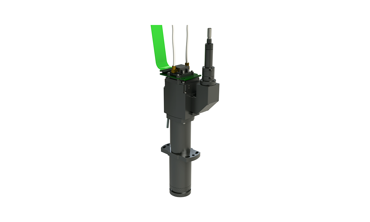
1.3X-2.7X 405nm DI Lithography System
1.3X-2.7X 405nm DI Lithography System
1.3X-2.7X 405nm DI Lithography System
Trace Photolithography
Trace Photolithography
Specifications
Key Technical Indicators
Specifications
Magnification
1.3X-2.7X
waves
405nm
Line Width Resolution
15-50um
Application Fields
Applied to PCB Trace Layer Exposure Photolithography Process, with Excellent Depth of Focus
Product Consultation
Submit
Copyright © BHOE All Rights Reserved.
九游平台
|
爱游戏网站首页_爱游戏(中国)
|
开云世界杯
|
乐鱼注册
|
星空平台
|
米兰官网入口_米兰(中国)
|
9U.COM九游体育(中国大陆)科技公司
|
世界杯官方认证平台_世界杯(中国)
|
华体会平台
|